

Their approach may remodel a scientific subject reliant on cost-prohibitive know-how.
Researchers on the Georgia Institute of Know-how have developed a light-based technique of printing nano-sized metallic constructions that’s considerably quicker and cheaper than any know-how at the moment accessible. It’s a scalable answer that would remodel a scientific subject lengthy reliant on applied sciences which might be prohibitively costly and sluggish. The breakthrough has the potential to carry new applied sciences out of labs and into the world.
Benefits of the New Method
Technological advances in lots of fields depend on the power to print metallic constructions which might be nano-sized — a scale a whole lot of occasions smaller than the width of a human hair. Sourabh Saha, assistant professor within the George W. Woodruff College of Mechanical Engineering, and Jungho Choi, a Ph.D. pupil in Saha’s lab, developed a way for printing metallic nanostructures that’s 480 occasions quicker and 35 occasions cheaper than the present typical technique.
Their analysis was printed within the journal Superior Supplies.
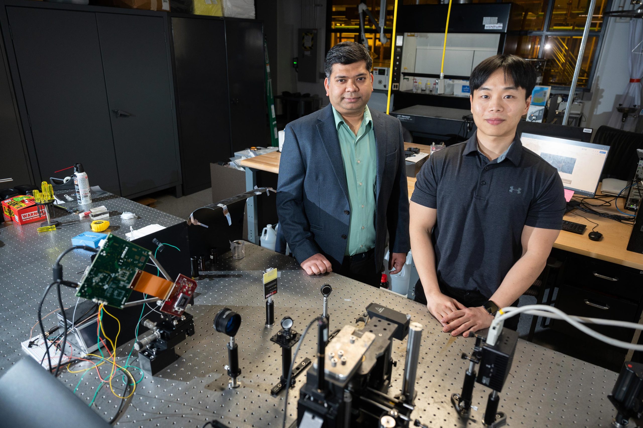
Assistant Professor Sourabh Saha and Jungho Choi (Ph.D. pupil) in entrance of their superluminescent mild projection system at Georgia Tech. Credit score: Georgia Institute of Know-how
Overcoming Conventional Limitations
Printing metallic on the nanoscale — a way generally known as nanopatterning — permits for the creation of distinctive constructions with attention-grabbing capabilities. It’s essential for the event of many applied sciences, together with digital gadgets, photo voltaic vitality conversion, sensors, and different methods.
It’s typically believed that high-intensity mild sources are required for nanoscale printing. However any such software, generally known as a femtosecond laser, can value as much as half 1,000,000 {dollars} and is just too costly for many analysis labs and small companies.
“As a scientific group, we don’t have the power to make sufficient of those nanomaterials shortly and affordably, and that’s the reason promising applied sciences typically keep restricted to the lab and don’t get translated into real-world functions,” Saha mentioned.
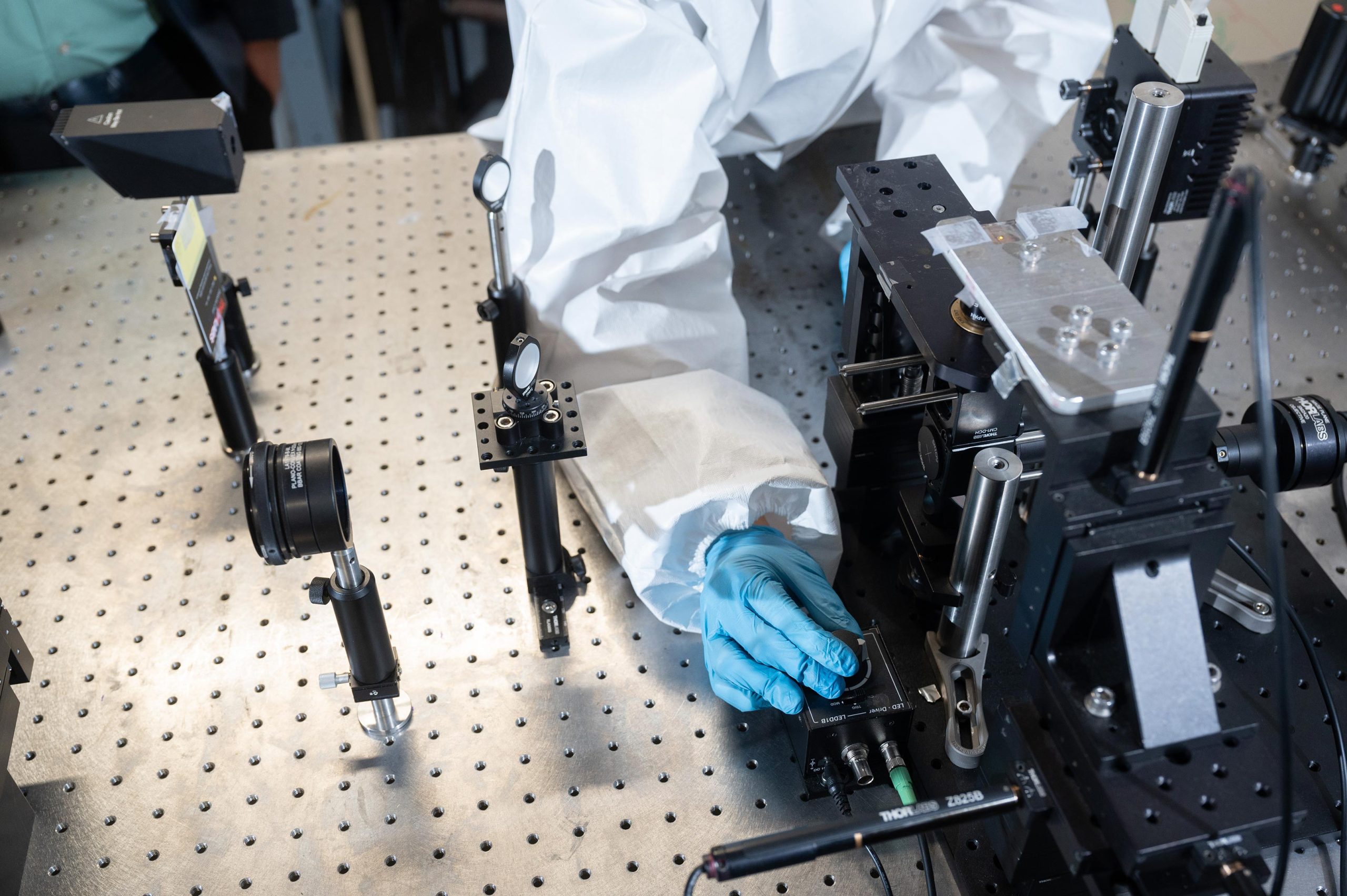
Ph.D. pupil Jungho Choi controlling LED brightness ranges on the SLP system. Credit score: Georgia Institute of Know-how
“The query we wished to reply is, ‘Do we actually want a high-intensity femtosecond laser to print on the nanoscale?’ Our speculation was that we don’t want that mild supply to get the kind of printing we would like.”
They looked for a low-cost, low-intensity mild that may very well be centered in a means just like femtosecond lasers, and selected superluminescent mild emitting diodes (SLEDs) for his or her industrial availability. SLEDs emit mild that may be a billion occasions much less intense than that of femtosecond lasers.
A video of nanoprinting with superluminescent mild projection (SLP). Credit score: Georgia Institute of Know-how
Progressive Printing Know-how
Saha and Choi got down to create an authentic projection-style printing know-how, designing a system that converts digital photos into optical photos and shows them on a glass floor. The system operates like digital projectors however produces photos which might be extra sharply centered. They leveraged the distinctive properties of the superluminescent mild to generate sharply centered photos with minimal defects.
They then developed a transparent ink answer made up of metallic salt and added different chemical substances to ensure the liquid may take in mild. When mild from their projection system hit the answer, it triggered a chemical response that transformed the salt answer into metallic. The metallic nanoparticles caught to the floor of the glass, and the agglomeration of the metallic particles creates the nanostructures. As a result of it’s a projection sort of printing, it may well print a complete construction in a single go, reasonably than level by level — making it a lot quicker.
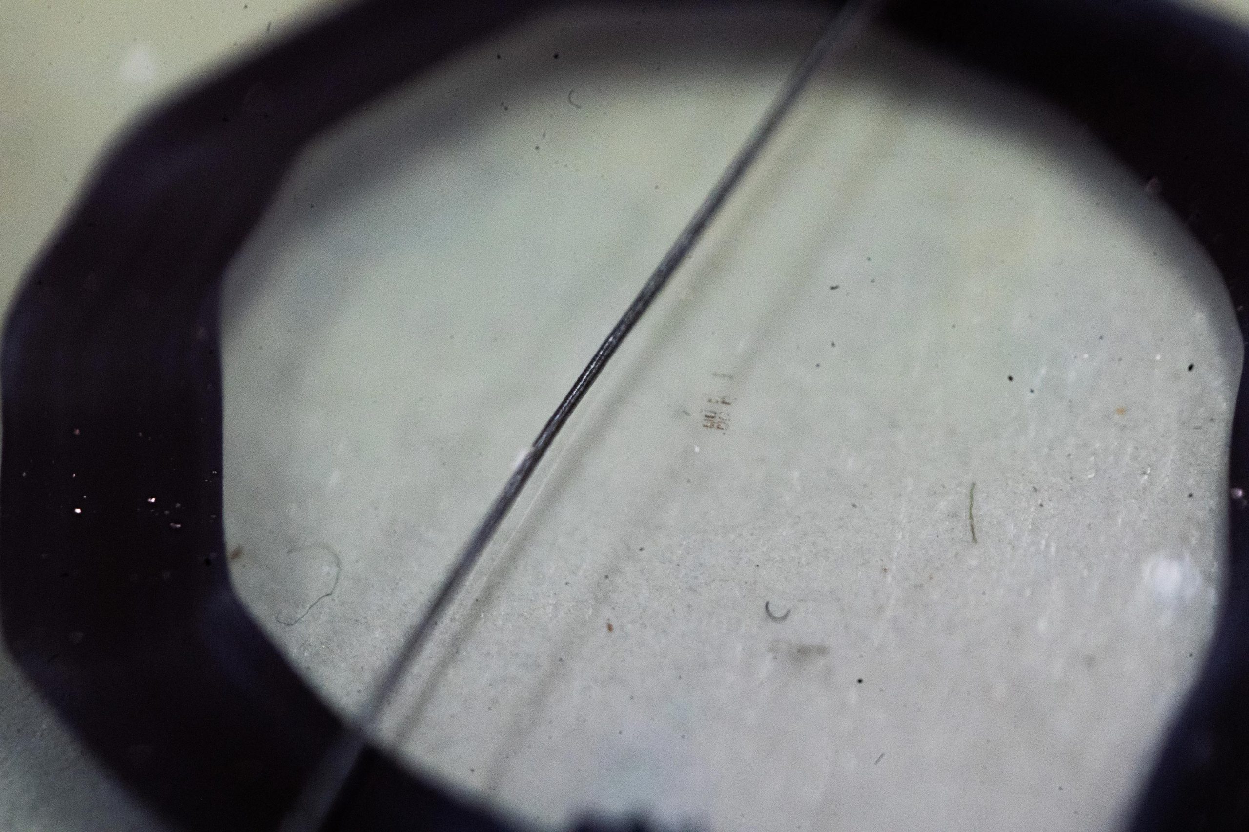
Dimension comparability between human hair (~100 micrometer thickness) versus printed silver pad on a glass coverslip. Credit score: Georgia Institute of Know-how
After testing the approach, they discovered that projection-style nanoscale printing is feasible even with low-intensity mild, however provided that the photographs are sharply centered. Saha and Choi imagine that researchers can readily replicate their work utilizing commercially accessible {hardware}. Not like a dear femtosecond laser, the kind of SLED that Saha and Choi used of their printer prices about $3,000.
Purposes
“At current, solely prime universities have entry to those costly applied sciences, and even then, they’re situated in shared services and aren’t at all times accessible,” Choi mentioned. “We need to democratize the potential of nanoscale 3D printing, and we hope our analysis opens the door for better entry to any such course of at a low value.”
The researchers say their approach will probably be significantly helpful for folks working within the fields of electronics, optics, and plasmonics, which all require a wide range of advanced metallic nanostructures.
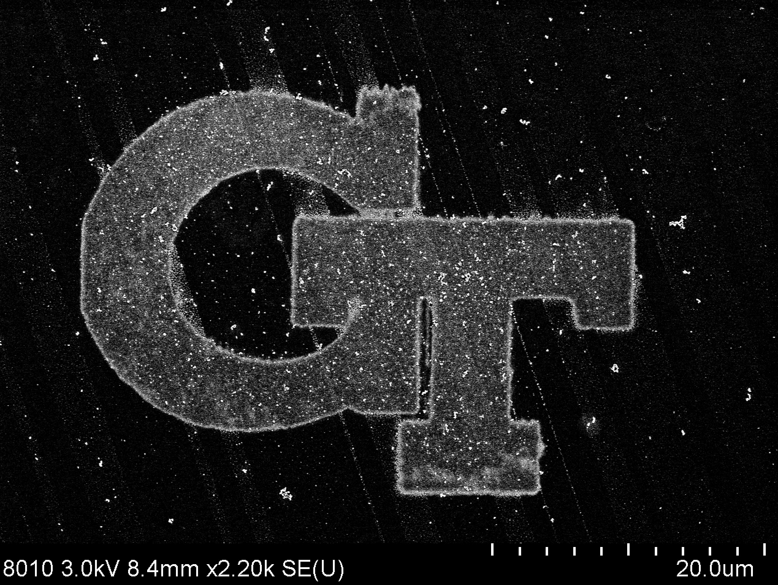
Scanning electron microscope picture of printed silver GT sample Credit score: Georgia Institute of Know-how
“I feel the metrics of value and pace have been significantly undervalued within the scientific group that works on fabrication and manufacturing of tiny constructions,” Saha mentioned.
“In the actual world, these metrics are vital on the subject of translating discoveries from the lab to trade. Solely when we now have manufacturing strategies that take these metrics into consideration will we be capable to absolutely leverage nanotechnology for societal profit.”
Reference: “Scalable Printing of Steel Nanostructures by means of Superluminescent Gentle Projection” by Jungho Choi and Sourabh Ok. Saha, 22 October 2023,Superior Supplies.
DOI: 10.1002/adma.202308112
Funding consists of grants from the G.W.W. College of Mechanical Engineering and the EVPR’s workplace on the Georgia Institute of Know-how. Imaging was carried out on the Georgia Tech Institute for Electronics and Nanotechnology, a member of the Nationwide Nanotechnology Coordinated Infrastructure (NNCI), which is supported by the Nationwide Science Basis (ECCS-2025462).