
Semiconductors are at all times within the information because the drive for higher capabilities in ever reducing bundle sizes. With the announcement of 3nm node units going into manufacturing, the challenges proceed to extend. TSMC has began a pilot manufacturing of 3nm units [Ref. 1]. The shrinkage in dimension is on the level the place there are wants for brand spanking new transistor designs. The path seems to be transferring from FinFET to a Gate-All-Round FETs design. Determine 1 is from reference 2.
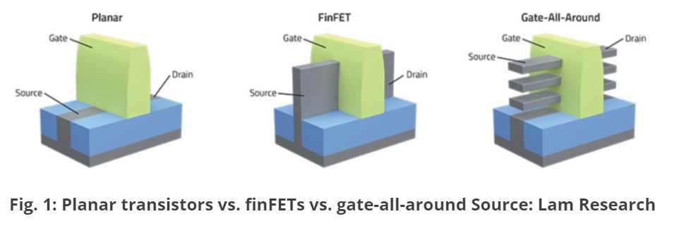
Clearly, there are manufacturing challenges. One of many proposed GAA FET designs is predicated on nanosheets of fabric. It seems that some manufactures will introduce the nanosheet FET at 3nm and others at 2nm. (Extra particulars on the event of the FETs might be present in reference 2.)
Analysis at Tsinghua College in Beijing, China have developed a transistor with atomically thinned channels which have a gate size of 0.34nm. [Ref. 3 & 4] That is nonetheless years from manufacturing prospects if it occurs in any respect. A number of applied sciences are developed, however a really restricted quantity are capable of be developed the place the method would work in quantity manufacturing. Nevertheless, this work signifies there a prospects for continued discount within the dimension of the transistors.
Researchers at Georgia Tech, Tianjin College, and Kwansei Gakuin College have demonstrated a nanoelectronics platform based mostly on graphene [Ref. 5]. The method employs e-beam lithography to attach the perimeters to silicon carbide units. If oxygen can connect with the graphene, it turns into graphane, which is an insulator.
There are different choices for bettering the efficiency capabilities of the semiconductor units. Chiplets [Ref. 6] are small components of a circuit that may be employed throughout a big number of units. The benefits of chiplets embody the power of co-locating processors with reminiscence instantly adjoining. This reduces the time it takes a sign to maneuver to or from reminiscence, which ends up in improved efficiency. However, nothing is with out challenges. Reference 7 covers the necessity for heterogeneous integration to create multi-die packages. The benefit of smaller space die/chips supplies the power to extend yields as a consequence of much less advanced particular person semiconductor capabilities.
There may be one other consideration when stacking chiplets. A single semiconductor die is constructed right into a bundle that dissipates warmth to maintain the system temperature from turning into too sizzling. Stacking a number of chiplets removes these parts of the circuitry away from a warmth sync. The buildup of warmth will influence efficiency and will have an adversarial influence on long-term system reliability.
All the efforts inside the semiconductor trade and researchers worldwide has coordination. Within the Nineties, the Worldwide Know-how Roadmap for Semiconductors (ITRS) was developed to offer steerage for researchers to handle future wants that might be required to be in manufacturing over the subsequent 10 to fifteen years. This roadmap was up to date yearly. The roadmap committee restructured the ITRS format to handle seven totally different expertise areas. The roadmap was renamed the Worldwide Roadmap for Gadgets and Techniques (IRDS) to extra appropriately handle the wants of the whole course of. The accountability of the IRDS was moved from the roadmap committee to the Institute of Electrical and Digital Engineers (IEEE). The main target of the IRDS remains to be the necessities for the subsequent fifteen years on a frequently transferring foundation. Extra particulars and the roadmap can be found is reference 8.
Adjustments are coming to semiconductor expertise that may enhance the efficiency of units and create new alternatives for innovate merchandise that require higher computing energy.
References:
- https://auto.economictimes.indiatimes.com/information/auto-components/tsmc-begins-pilot-production-of-3nm-chips/88071568
- https://semiengineering.com/new-transistor-structures-at-3nm-2nm/
- https://www.tomshardware.com/information/semi-transistors-atom-thick
- https://www.nature.com/articles/s41586-021-04323-3
- https://www.graphene-info.com/researchers-take-step-towards-graphene-electronics
- November 2022 Weblog http://www.nano-blog.com/?m=202211
- https://semiengineering.com/heterogeneous-integration-co-design-wont-be-easy/
- https://irds.ieee.org